7. Hardware Specification
This section describes the hardware specifications of the MN-Core 2 that are particularly relevant to MLSDK users. For more detailed information, please refer to the following software developer manuals:
7.1. Hierarchical Architecture
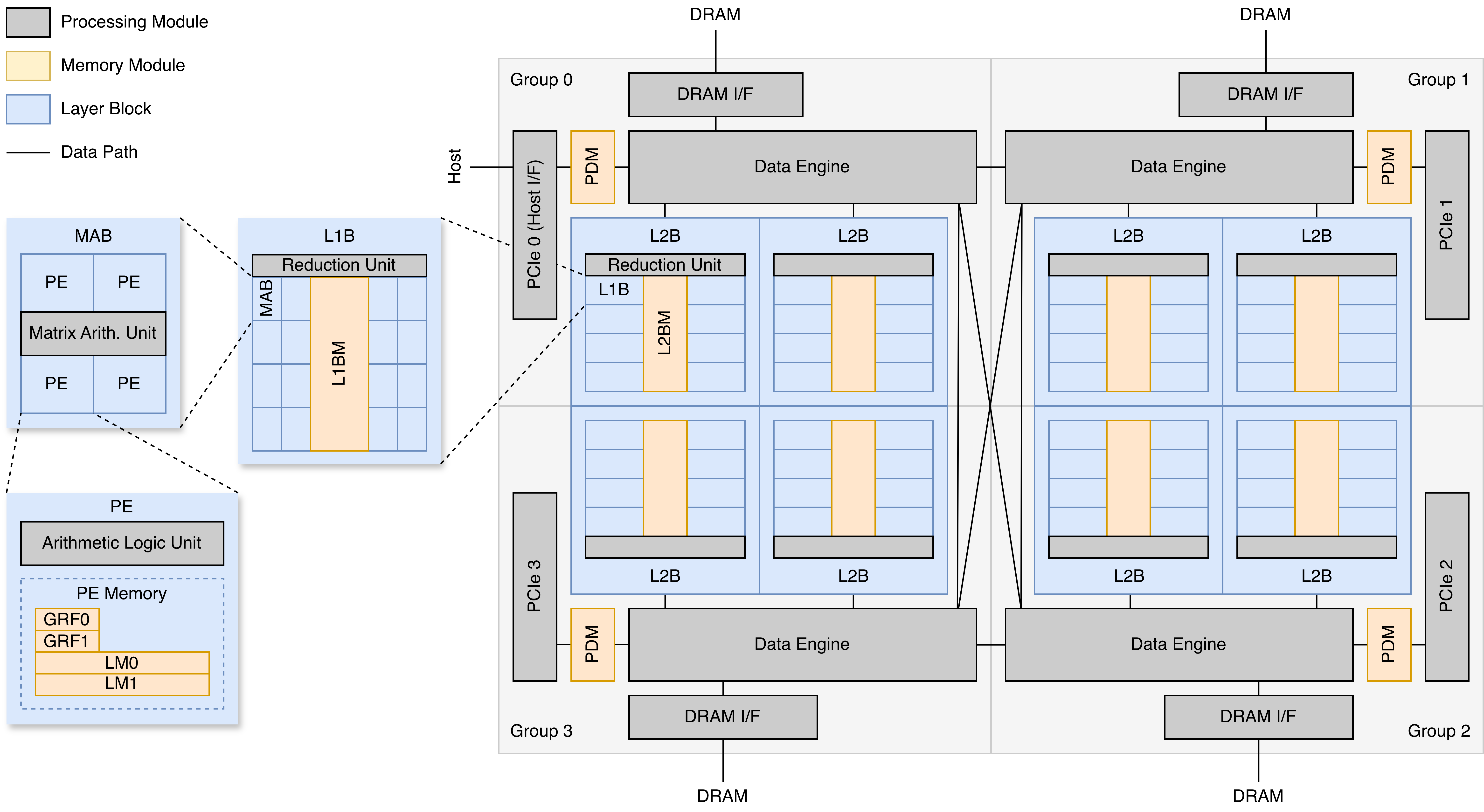
Fig. 7.1 MN-Core 2 hierarchical architecture consisting of the multiple layer blocks.
Note: this is a schematic representation and does not reflect the physical floorplan of the chip.
We explain the distinctive hierarchical memory and processing unit architecture of the MN-Core 2, as illustrated in Fig. 7.1. As a design principle, processing units are positioned at the leaf nodes of the tree structure, while large-capacity local memory is installed adjacent to them. This configuration enables efficient processing of operations with high spatial locality. Additionally, the memory at the intermediate hierarchical levels - corresponding to the tree’s internal nodes - is significantly smaller than local memory and is designed with a different approach compared to cache memory.
7.1.1. Overview of Each Hierarchical Level
The root of the tree structure is called the Top Level, from which branches extend to Group and L2B (Level 2 Block) levels.
- Top Level
Contains 4 Group units as child nodes.
Appears only once per board (comprising a single chip plus peripheral circuits).
A virtual grouping of 4 Group units, with no physical existence
- Group
Contains 2 L2B units as child nodes and includes one DRAM and one PDM.
The DRAM is counted as a single unit because it provides a single memory space by combining multiple modules.
Data transfer between L2B, DRAM and PDM at Top Level is achieved through the coordinated operation of Data Engine in each Group.
The role of the PDM will be explained later.
- L2B (Level 2 Block)
Contains 8 L1B units as child nodes.
- L1B (Level 1 Block)
Contains 16 MAB units as child nodes.
- MAB (Matrix Arithmetic Block)
Contains 4 PE units as child nodes.
- PE (Processing Element)
Contains several PE memories as child nodes.
In total, there are 4096 Processing Elements (PE) per board. Since the Top Level and Group levels share overlapping functions, we sometimes represent the configuration with 8 L2B directly under the Top Level for clarity.
7.1.2. Processor Units at Each Hierarchical Level
- MAU (Matrix Arithmetic Unit)
Matrix processing units contained within each MAB.
- ALU (Arithmetic Logic Unit)
Integer processing units contained within each PE.
- Inter-Level Reduction Units
Processor units used in data reduction pathways from lower to higher levels.
7.1.3. Memory Types at Each Hierarchical Level
We use LW (64-bit word) as the unit of memory capacity. For detailed specifications, please refer to the Memory Word section below.
- DRAM
High-capacity external memory accessed via the Top Level.
Each Group has its own memory space, with a total of 16 GiB capacity across 4 Groups.
The memory capacity per Group is 4 GiB.
- PDM (PIU Data Memory, PIU: PCIe Interface Unit)
Memory primarily used for DMA communication but can also be utilized as temporary memory.
Each Group has its own memory space, with a capacity of 4 MiB (= 512 Ki LW) per Group.
Only PDM in Group 0 is physically connected to the Host via the PCIe interface. All host-device communications pass through this PDM.
- L2BM
Memory contained within each L2B, with a capacity of 32 Ki LW.
- L1BM
Memory contained within each L1B, with a capacity of 8 Ki LW.
- PE Memory
General term for memory contained within each PE.
LM (Local Memory): Consists of two sides (LM0/LM1), each with a capacity of 2 Ki LW.
GRF (General Register File): Consists of two sides (GRF0/GRF1), each with a capacity of 256 LW.
Note
This document intentionally omit the description of T-Register in the PE Memory for consistency. For more information, please refer to the software developer manual.
Note
In the MLSDK, memory selectable as Location is limited to DRAM and LM0/LM1. Other memory types are primarily used for scratchpad purposes or as buffers for data transfer operations.
7.2. Memory Word
For on-chip memory in MN-Core 2, there are three standard units of memory elements:
LW (Long Word): 64-bit word
SW (Single Word): 32-bit word
HW (Half Word): 16-bit word
Among these, SW corresponds to the minimum addressable unit for PE memory (GRF0, GRF1, LM0, LM1), and address notation in assembly also uses SW units. However, due to alignment constraints, data transfer operations must be performed in LW or larger units, hence LW is primarily used for element count notation. Regarding HW, since it is essentially a unit used internally by the arithmetic units, in assembly it is handled in groups of 2 or 4.
The address units used for each memory element within MN-Core 2 (assembly operands within parentheses) are summarized as follows:
- LW unit
DRAM (
$d), PDM ($p), L2BM ($lc), L1BM ($lb)- SW unit
LM0 (
$m), LM1 ($n), GRF0 ($r), GRF1 ($s)- HW unit
(None)
Note
The operand access word length specification, long word ($l) and double long word ($ll), has no direct relationship with address units. For example, the $m8, $lm8, and $llm8 with different specifications will all start reading from the same address. Instead, by setting respective address increment widths to 1, 2, and 4, continuous memory regions can be accessed without overlap.
Note
In relation to Layout, the following summarizes the correspondence with word lengths in Layout notation.
Memory addresses in Layout are expressed in LW units, with the number of elements contained in one LW indicated by _W.
For example, for a 12-element tensor with shape=(12,), when the dtype is double precision (LW), single precision (SW), or half precision (HW), the corresponding Layout would be as follows:
LW:
(12,)/((12:1); B@[W,...])(Note that1_Wis represented asB@[W])SW:
(12,)/((6:1, 2_W:1); B@[...])HW:
(12,)/((3:1, 4_W:1); B@[...])
Even for the same number of elements, using lower precision results in less memory consumption, which is reflected in smaller address sizes.
7.3. Floating Point Format
The floating point number formats in MN-Core 2 are as follows:
Precision |
Sign bit |
Exponent bit |
Mantissa bit |
|---|---|---|---|
Half precision (HW) |
1 bit |
6 bit |
9 bit |
Single precision (SW) |
1 bit |
8 bit |
23 bit |
Double precision (LW) |
1 bit |
11 bit |
52 bit |
Representative values |
Half precision (1-6-9) |
Single precision (1-8-23) |
Double precision (1-11-52) |
|---|---|---|---|
+0.0 |
0x0000 |
0x00000000 |
0x0000000000000000 |
-0.0 |
0x8000 |
0x80000000 |
0x8000000000000000 |
+1.0 |
0x3E00 |
0x3F800000 |
0x3FF0000000000000 |
Maximum positive normalized number |
0x7DFF |
0x7F7FFFFF |
0x7FEFFFFFFFFFFFFF |
Maximum positive normalized number (real value) |
4.29077e+09 |
3.40282e+38 |
1.79769e+308 |
Minimum positive normalized number |
0x0200 |
0x00800000 |
0x0010000000000000 |
Minimum positive normalized number (real value) |
9.31323e-10 |
1.17549e-38 |
2.22507e-308 |
Positive infinity |
0x7E00 |
0x7F800000 |
0x7FF0000000000000 |
Only normalized numbers, positive/negative zeros, and positive/negative infinity can be represented. Non-normalized numbers and NaN values cannot be represented. Accordingly, when the exponent field is all 0s regardless of the mantissa value, it represents a positive or negative zero, and when all 1s, it represents positive or negative infinity. All other values are normalized numbers, and their interpretation follows IEEE 754 standards within their respective ranges.
In Dtype, the Half, Float (Float32), and Double types correspond to the above half-precision, single-precision, and double-precision formats, respectively.
Note
There are block floating-point and pseudo-single precision formats primarily used in matrix-vector dot product operations. For detailed information on these formats, please refer to the software development manual. Since operation results are converted to the original formats mentioned above, they generally do not correspond to Dtype.